

Identifying Critical Thermal Hotspots in PCB Development With IR Cameras
Optimizing PCB Layouts with Thermal Imagers
Challenge
Managing heat in high power density PCBs is difficult due to limited space, large heat-generating components, and the risk of thermal spikes from poor layout. Traditional contact methods fail to provide comprehensive thermal data, making it hard to detect and address hotspots effectively during the design phase.
Solution
Infrared cameras enable full-surface thermal visualization of powered PCB prototypes, allowing engineers to detect and address hotspots early. This non-contact method supports accurate analysis and design adjustments, ensuring optimal thermal distribution without interfering with board performance or requiring extensive physical sensors.
Benefits
- Improves reliability by identifying hotspots before finalizing the board layout
- Reduces failure risks and costly recalls through early thermal optimization
- Speeds up development with efficient, in-lab thermal testing iterations
- Cuts costs by eliminating extensive thermocouple setups and labor
- Enables informed design decisions with comprehensive, real-time thermal data
Addressing Thermal Risks in PCB Development
Controlling heat generation in high power density printed circuit boards (PCBs) is challenging due to the simultaneous power draw from numerous traces and the reliance of multiple components on a consistent current supply. High power density is often necessary for applications requiring various functions. Efficient space utilization is crucial, as any crosstalk can rapidly lead to thermal spikes.
Additionally, some high power density PCBs incorporate large components, adding complexity to thermal management. Larger components generate more heat and reduce the available surface area for dissipation. Ensuring sufficient area for heat dissipation is essential for proper cooling. Crowding components, even if compliant with IPC standards, can be counterproductive.
Effective thermal management is vital in PCB design, significantly affecting the physical performance and functionality of the board. Therefore, it should be a priority for every designer. Identifying and mitigating hotspots is critical to ensure the reliability and safety of the final product. Hotspots can indicate areas where components are improperly placed or at risk of overheating, leading to component failure or fires. This challenge was highlighted by a case where a customer experienced a series of failures due to overheating in the field, prompting the need for more effective thermal analysis during the design phase. Traditional methods like using thermocouples proved insufficient due to their inability to cover the entire board comprehensively and the physical interference they introduced. The need for a non-contact, comprehensive solution led to the exploration of infrared cameras.
Using IR Cameras for Effective Thermal Analysis to Optimize PCB Layouts
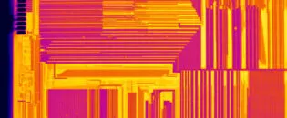
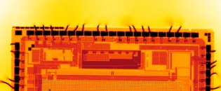
In PCB development, IR cameras provide a significant advantage by enabling engineers to visualize thermal distribution across the entire board. This capability is crucial for the early identification of potential hotspots, which can be addressed through component repositioning or design adjustments. Without the ability to detect these thermal anomalies, PCBs are at a higher risk of failure, leading to costly recalls and damage to the company’s reputation. Thus, the motivation for integrating advanced thermal imaging solutions, like those offered by Optris, stems from the need for enhanced safety, efficiency, and reliability in PCB production.
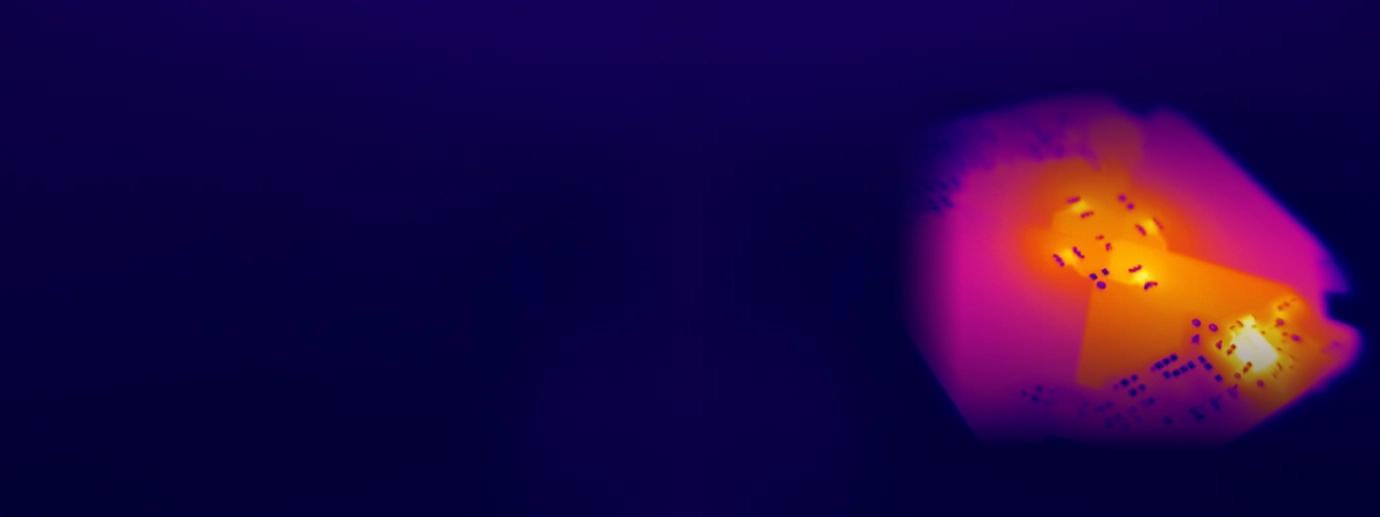
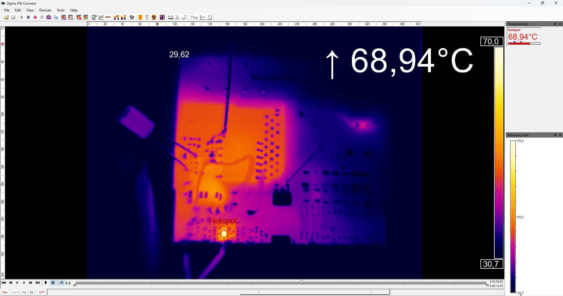
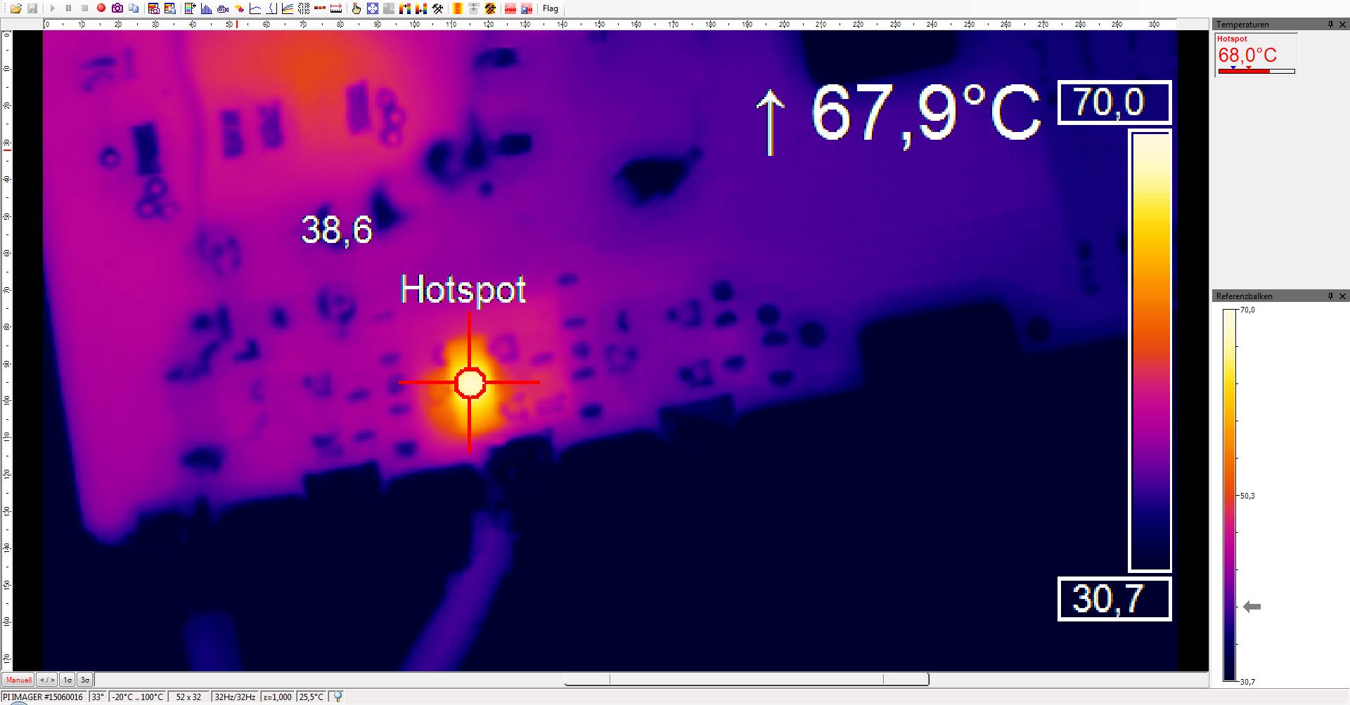
Engineers utilize Optris IR cameras to monitor the thermal performance of prototype boards, pinpointing areas of excessive heat buildup by powering the boards and observing the thermal images. Optris thermal imagers, such as the PI 450i and PI 640i, are particularly effective due to their high resolution and ability to capture detailed thermal profiles. These cameras allow engineers to see the exact location and intensity of hotspots, facilitating precise adjustments to the board design.
During testing, thermal cameras are set up in a laboratory environment where electrically powered prototypes undergo thorough thermal analysis. Engineers capture real-time thermal data, which is then analyzed to determine if any components generate excessive heat. If a hotspot is detected, the layout is redesigned to improve thermal distribution. This iterative process continues until the board’s thermal performance meets the required standards. Using Optris thermal cameras, engineers can ensure that all components operate within safe temperature ranges, significantly reducing the risk of thermal-related failures.
Additionally, implementing thermal cameras replaces the need for extensive use of thermocouples, which are labor-intensive to install and provide limited data. Infrared cameras offer a non-invasive alternative that delivers comprehensive thermal data without altering the board’s thermal characteristics. The software capabilities of Optris cameras further enhance this process by allowing detailed analysis and documentation of thermal profiles, making it easier for engineers to communicate findings and make informed design decisions.
Benefits of Optris Solutions in PCB Testing
Thermal analysis through IR cameras enhances the reliability and safety of the final product. By identifying and mitigating hotspots early in the design phase, engineers can prevent potential failures and ensure that the boards perform optimally under operating conditions. This proactive approach reduces the likelihood of recalls and field failures, protecting the company’s reputation and saving costs associated with warranty claims and repairs. The detailed thermal data, combined with the advanced capabilities of Optris cameras, ensures that engineers can address thermal issues early, optimize component placement, and ultimately deliver high-quality, reliable PCBs.
Moreover, the use of Optris infrared cameras significantly streamlines the testing process. The high-resolution images provided by these cameras offer a clear and detailed view of the thermal distribution, making it easier to pinpoint issues and implement solutions quickly. This efficiency not only accelerates the development cycle but also allows for faster time-to-market for new products. The ability to test and validate designs in-house also enhances the overall design quality, as engineers have greater control over the testing environment and can iterate more rapidly.
Another significant benefit is the cost savings achieved through the reduction in physical testing components like thermocouples. By relying on non-contact thermal imaging, companies can minimize the resources and labor required for thermal analysis, leading to more efficient use of engineering time and budget. Moreover, the comprehensive data provided by Optris cameras supports better decision-making and documentation, which is crucial for maintaining high standards in PCB manufacturing.
Recommended Products


Other Electronics Applications


Talk to us about your IR Temperature Measurement Requirements
There are over 300 different pyrometer variants to choose from in the Optris infrared pyrometer portfolio each optimized for material, spot size, distance from the target, and environmental conditions. Fortunately, there is a trained engineer to phone or chat with to guide you through the process of choosing the perfect infrared sensor for your application.
The same support is available for the extensive IR camera product line.
