

Microthermography Research on Next-Generation MEMS and Microprocessors
Achieving High Resolution Thermal Analysis for Complex ICs and MEMS in Advanced Microelectronics
Challenge
Miniaturized electronics and MEMS increasingly face localized overheating due to dense circuitry and layered packaging, making thermal validation difficult. Detecting microscopic defects and hotspots non-invasively in complex structures is challenging, especially when subsurface analysis is required without damaging delicate components.
Solution
Infrared microthermography enables precise, non-contact thermal analysis of microelectronics, visualizing surface and subsurface temperature variations in real time. This technique supports failure analysis and defect localization with high spatial and thermal resolution, even under electrical excitation, ensuring thermal optimization throughout the design and validation stages of miniaturized components.
Benefits
- Visualizes thermal behavior of MEMS and microelectronics with microscopic spatial resolution.
- Identifies thermal defects and hotspots early during design and validation stages.
- Supports real-time, non-destructive testing under electrical excitation or dynamic load conditions.
- Enables accurate analysis of temperature gradients in complex packaging and IC structures.
- Enhances yield and reliability by preventing overheating and thermal-related device failure.
Advancing Miniaturization: Thermal Optimization for Next-Generation Microelectronics and MEMS with Microthermography
Thermal optimization when developing new microelectronic products becomes more challenging and important. Microelectromechanical systems (MEMS) have vast potential applications in nanotechnology, with common examples including position recognition in mobile phones, and their use in airbags, digital cameras, and pacemakers. Micro-Electro-Mechanical Systems (MEMS) technology is also increasingly utilized in miniaturized medical diagnostics, offering new possibilities for advanced healthcare solutions. The push for miniaturization affects not only the system solutions required but also the development of sensors and control elements. As complex electronics continue to shrink while increasing in power, effective thermal management becomes ever more critical.
Modern microprocessors, with their densely integrated circuits and transistors, face challenges from localized hotspots that can degrade performance and reduce lifespan. Thermal validation is particularly difficult in detecting these hotspots, especially when they are embedded beneath multiple metal layers or in flip-chip packages.
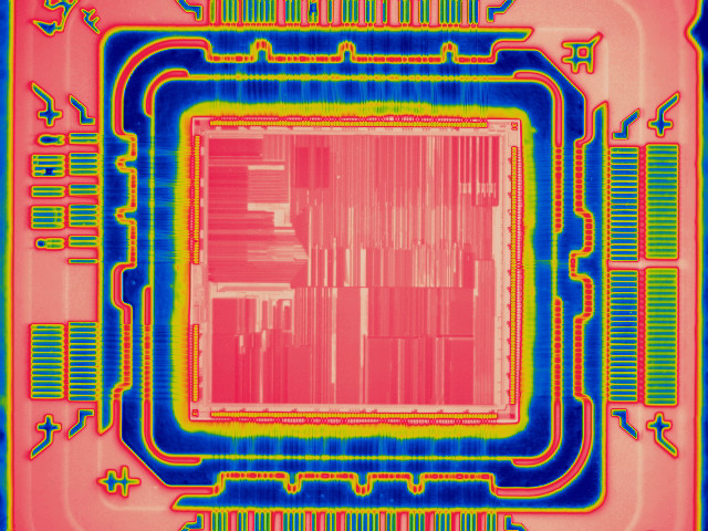
Microthermography, which provides highly accurate thermal analysis at the micrometer scale, offers detailed insights into the temperature distribution of intricate electronic assemblies and components, ensuring optimal performance and reliability. These advanced thermal imaging systems enable precise analysis of temperature distribution in energized components, effectively identifying and tracking hotspots within the image area. As microprocessor technology advances, increasing performance and reducing die costs, the number of metal layers, CMOS devices, and interconnect density in integrated circuits (ICs) continues to grow. This trend in sub-micron technology complicates defect localization. Infrared microscopy presents a significant advantage in this area, as intrinsic silicon becomes nearly transparent at wavelengths beyond its 1.1µm bandgap. Although dopants increase silicon’s absorption, this effect only becomes significant in heavily doped substrates, making infrared microscopy a powerful tool for analyzing complex electronic structures.
Traditionally, high performance infrared imaging system, particularly those sensitive to the mid-infrared range from 2 – 5µm, offer non-invasive, real-time imaging of thermal emissions from these critical areas. Nevertheless, they have several disadvantages, including high cost, bulkiness, consume more power, and the need for cryogenic cooling systems, which increase maintenance complexity.


Affordable High-Precision Infrared Microscopy unravels Microprocessor Thermal Fingerprint
Infrared microscopy, particularly with advanced tools like the PI 640i infrared microscope kit with 2X magnification, provides a precise solution for engineers requiring detailed thermal analysis of small electronic devices or MEMS. This infrared imaging system allows research and design engineers to visualize thermal variations and accurately measure temperature on minute targets, utilizing high-resolution detector technology to focus infrared heat energy onto the camera’s sensor. This capability ensures reliable and detailed thermal analysis of even the smallest components, making it ideal for non-destructive failure analysis of microprocessors, MEMS, microelectronics, and packaging systems.
Unlike cooled infrared microscopes, which are magnitudes more expensive, the PI640i microscope with 2X magnification works in the long infrared wavelength domain from 8-14µm. Modern microbolometers, which do not need to be cooled, can detect this wavelength region. This allows engineers to have access to infrared imaging technology at a much smaller budget.
High-resolution infrared cameras, such as the PI 640i, offer a field of view of 5.4 mm x 4.0 mm and can detect temperature changes on targets as small as 8 µm (IFOV), which is close to the difrraction limitation at the mentioned wavelength. Combined with low thermal noise and an optimal pixel pitch size of 17 µm, allow for small Measurement Field of View (MFOV) requirements of just 4 x 4 pixels. The PI 640i supports a frame rate of 32 Hz in standard mode or 125 Hz in high-speed subframe mode, enabling engineers to monitor rapid thermal processes in real time.
This advanced non-contact thermal analysis system reliably detects and analyzes even the smallest defects and thermal inconsistencies, supporting high-resolution testing and validation of modern microprocessors, MEMS, and other miniaturized electronics.
Advanced Defect Detection in Microelectronics with The Power of Dark Lock-In Thermography
The PI640i infrared imaging system boasts a low NETD, making it highly sensitive to small temperature variations. The lock-in principle, or lock-in amplification, is employed to extract useful signals from a noisy background, particularly in applications where voltages are applied to the device under test (DUT) to reveal its thermal signature. In certain cases, Dark Lock-In Thermography (DLIT) is applied for more precise defect analysis. When using DLIT, the DUT is connected to a power supply, and its heat emissions are measured using an infrared camera to detect localized areas of poor quality through surface temperature analysis.
In DLIT, a pulsed voltage is applied to the DUT, and the resulting temperature modulations are captured. This non-destructive imaging technique is particularly effective for identifying and analyzing electrical defects in microelectonic devices. DLIT operates by modulating heat sources with a periodic signal under an applied electrical bias, allowing the infrared camera to detect subtle temperature oscillations.
By periodically pulsing heat into the sample and observing the stimulated surface’s temperature field, the method targets both heating and cooling curves. This is typically achieved by toggling the supply voltage or using sinusoidal modulation, revealing localized cooling processes after each excitation pulse. This approach allows for the detection of subsurface structures, making it particularly valuable in applications such as power semiconductor assembly.
DLIT can detect weak currents and fine thermal details, highlighting areas where electrical imperfections, such as excessive recombination of charge carriers, cause heat generation. The periodic modulation enhances both sensitivity and spatial resolution, enabling detection of temperature variations below the NETD threshold, down to microkelvin levels. This capability makes it an essential tool for identifying even the smallest thermal anomalies.
Recommended Products


Other Electronics Applications


Talk to us about your IR Temperature Measurement Requirements
There are over 300 different pyrometer variants to choose from in the Optris infrared pyrometer portfolio each optimized for material, spot size, distance from the target, and environmental conditions. Fortunately, there is a trained engineer to phone or chat with to guide you through the process of choosing the perfect infrared sensor for your application.
The same support is available for the extensive IR camera product line.
