

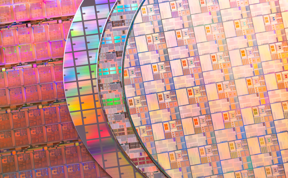
Rapid Thermal Annealing of Wafers Requires Infrared High-Temperature Monitoring
Control Rapid Thermal Annealing in Semiconductor Manufacturing with Infrared Temperature Sensors
Challenge
Rapid thermal annealing demands precise, uniform wafer heating above 1000°C within seconds while managing silicon’s varying emissivity across wavelengths and temperatures. Conventional infrared methods struggle with interference from heat lamps, transparency at lower temperatures, and maintaining accuracy in harsh conditions, complicating reliable in-situ thermal monitoring.
Solution
Employing infrared ratio pyrometers with fiber-optic sensing heads ensures accurate, non-contact wafer temperature measurements, overcoming emissivity variations and optical interferences common in rapid thermal processing. The approach facilitates precise monitoring in challenging conditions, ensuring uniform heating without contamination, thus optimizing semiconductor production efficiency and quality.
Benefits
- Precise, uniform wafer heating improves electrical properties, reducing defects and increasing yield.
- Real-time monitoring enables rapid detection and correction of temperature deviations during processing.
- Non-contact measurement prevents contamination risks, maintaining wafer purity and process integrity.
- Reliable temperature control reduces thermal stress, minimizing wafer breakage and production downtime.
- Cost-efficient temperature monitoring solution accelerates development cycles, enhancing overall manufacturing productivity.
Rapid Thermal Annealing for Stress Relief requires Infrared High-Temperature Monitoring
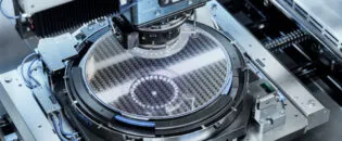
Thermal annealing, a key semiconductor manufacturing method, involves heating wafers to high temperatures to modify their electrical properties and relieve stress in silicon. Rapid thermal processing, a crucial part of this method, is instrumental in achieving dopant activation and crystal repair without significant diffusion, thereby enhancing the efficiency of the process.
Conventionally, thermal annealing processes were often performed using conventional resistive-heated tube furnaces in an inert ambient. The normal temperature range for annealing processes lies between 900 °C and 1100 °C. For polysilicon anneal, the lower limit is extended to about 700 °C. A furnace anneal process for dopant activation and crystal damage repair might require 30 minutes at 900 °C.
Rapid thermal annealing (RTA), also known as rapid thermal processing, represents a significant advancement. It heats silicon wafers to temperatures exceeding 1000 °C for a few seconds, followed by slow cooling to prevent thermal shock and wafer breakage. This information keeps you informed and up-to-date in your field.
Various facilities employ different heat treatment methods, such as quartz tube lamps, induction heating, and resistance coating.

Navigating Silicon’s Emissivity and Thermal Uniformity in Rapid Thermal Processing
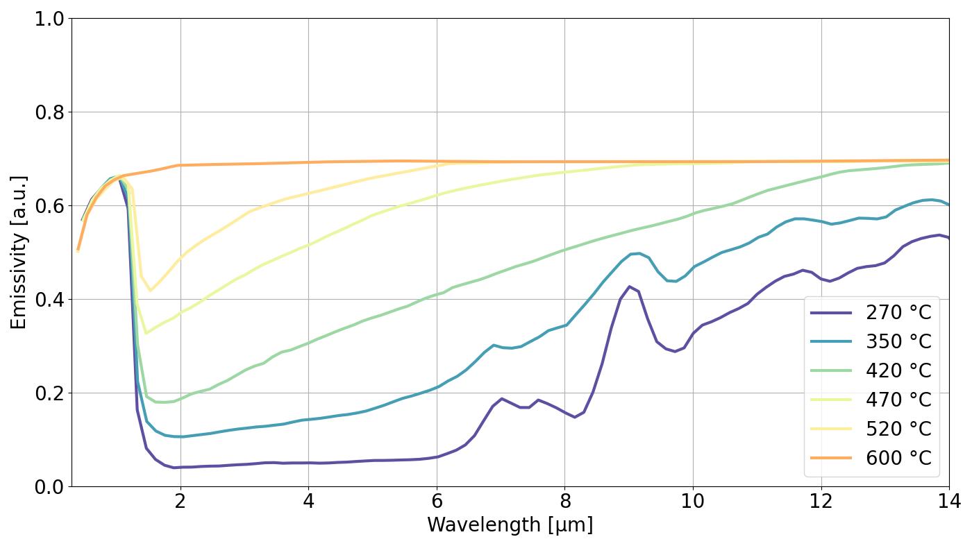
Silicon’s emissivity varies with temperature, wavelength, and surface characteristics, resulting in complex behavior across different spectral ranges.
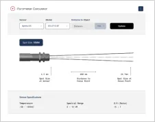
For equipment utilizing induction or resistance heating, in-situ and in-line temperature monitoring of semiconductor processes is often achieved with CTratio pyrometers. These compact, two-piece devices with flexible optical fibers can be positioned in confined or hard-to-reach areas. They are designed to withstand harsh conditions, including ambient temperatures up to 315 °C, vibrations, and chemical exposure.
Ratio technology provides precise temperature measurements by comparing the intensities of two different wavelengths of light, reducing errors caused by emissivity variations, optical interferences, or obstructions in the optical path. The smart ratio software mode can adjust for changes in silicon emissivity, ensuring accurate readings even when emissivity does not change uniformly at the two wavelengths.
Despite these advanced techniques, the semiconductor industry often uses heat lamps or places wafers near heated thermal masses. These facilities using quartz tube lamps benefit from silicon’s high emissivity at specific wavelengths but face challenges in accurate temperature measurement. The lamps emit energy around 1 µm, complicating infrared sensor detection as the sensors may pick up the quartz tube instead of the wafer. Silicon is transparent to long-wavelength infrared at low temperatures but becomes opaque at high temperatures. In such applications, pyrometers operating around 1 µm are inadequate, necessitating conventional long-wavelength infrared sensors. Multiple pyrometers or an infrared camera in a line scanner mode can be used for thermal uniformity measurement through a slit.
Optimizing Semiconductor Processes with Optris Pyrometers and Superior Technical Support
The fiber-optic CTratio with a passive sensing head offers significant advantages for installation in challenging environments. By keeping the electronics away from the harsh conditions of the reactor, this technology ensures both durability and longevity. The non-contact measurement system avoids interference with the process, eliminating any risk of contamination. Given the extremely high temperatures and potentially hazardous atmosphere, fiber-optic technology is crucial for maintaining accurate and safe temperature measurements.
The Optris pyrometer is both reliable and highly cost-effective, providing accurate and consistent temperature data at half the price of competing products. This makes it an economical choice without compromising performance. Additionally, the shorter lead time for the infrared sensor allows for quicker implementation and development cycles. Optris’s ongoing technical support ensures prompt resolution of any issues, enabling customers to rely on their expertise for continuous process optimization. This comprehensive approach not only guarantees immediate success but also fosters long-term partnerships.
Recommended Products


Other Semiconductors Applications


Talk to us about your IR Temperature Measurement Requirements
There are over 300 different pyrometer variants to choose from in the Optris infrared pyrometer portfolio each optimized for material, spot size, distance from the target, and environmental conditions. Fortunately, there is a trained engineer to phone or chat with to guide you through the process of choosing the perfect infrared sensor for your application.
The same support is available for the extensive IR camera product line.
