

Visualize the Invisible: Infrared Imaging for Superior Wafer Cleaning for Lithography Process
Leveraging Thermal Contrast to Detect and Remove Residues in Strip and Clean Process of Wafers
Challenge
Residual photoresist and contaminants can disrupt precise pattern transfer, causing defective circuits, impairing material deposition and etching processes, and ultimately reducing yield and device reliability. Visual detection methods are insufficient, making residues challenging to identify and remove thoroughly, risking process integrity and increasing production defects.
Solution
Infrared imaging leverages thermal contrasts between residues and wafer surfaces, allowing precise detection of otherwise invisible contaminants. This enables targeted cleaning, ensuring thorough removal of photoresist remnants. High-resolution infrared imaging specifically facilitates the identification of minute residues, significantly improving cleanliness and subsequent lithography performance.
Benefits
- Reduced defects through precise residue detection, enhancing yield and integrated circuit reliability.
- Improved process control by visualizing contaminants invisible to traditional inspection methods.
- Enhanced documentation of cleaning processes, enabling continuous quality and procedural improvements.
- Increased efficiency with targeted cleaning, saving valuable time and reducing production downtime.
- Early identification of contamination, minimizing costly rework and maximizing production throughput.
The Importance of Thorough Wafer Cleaning and Removal of Residual Photoresist
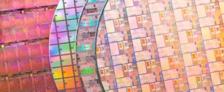
Optical lithography is a process used in the manufacturing of integrated circuits. It begins with applying a photosensitive material, known as photoresist, onto the substrate. A photomask containing the desired pattern is then positioned over the photoresist, and light is shone through the photomask, exposing specific areas of the photoresist. These exposed areas undergo a chemical change, becoming either soluble or insoluble in a developer solution. After development, the pattern is transferred onto the substrate through etching, chemical vapor deposition, or ion implantation.
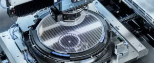
Once the structures are etched or deposited on the wafer, removing the photoresist and thoroughly cleaning the wafer is crucial. This cleaning process typically occurs in three distinct phases. Initially, the photoresist is stripped away. Subsequently, any remaining residues on the wafer surface are eliminated using specialized chemical cleaning methods. Finally, the surface is meticulously cleaned and passivated to prepare it for subsequent processing steps.
Several issues can arise if the wafer still contains photoresist before the following lithography process. Residual photoresist can result in inaccurate pattern transfer during subsequent lithography steps, leading to defective circuits or features on the wafer. Unclean wafers can introduce contaminants that interfere with material deposition, etching processes, or other manufacturing steps, potentially causing poor device performance or failure. Additionally, contaminated or improperly cleaned wafers can increase the rate of defects, reducing the overall yield of functional integrated circuits from the production batch.
An imaging method is necessary to detect residues of the API film or contamination in unknown positions during the cleaning process since they are not always visible in the visual spectral domain.


Infrared Imaging Reveals Wafer Residual Remnants of Photoresist
Infrared cameras are highly effective tools for this purpose, as they can make these particles, defects, or remnants visible.
Infrared cameras operate by detecting objects’ thermal emissions. Due to the different emission behaviors of residues and chemical cleaning agents used, the IR camera captures a thermal contrast that is not detectable in the visual spectral range. This thermal contrast highlights areas with residues or contaminants, allowing for precise identification and targeted cleaning. A high-resolution infrared camera is crucial because it provides detailed imaging to detect the wafer’s smallest residues and contaminants. High resolution enhances the infrared camera’s ability to capture fine details, making it possible to identify tiny particles that lower-resolution infrared cameras might miss.
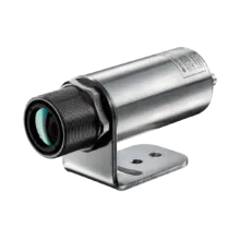
The Pi 640 infrared camera is a high-performance thermal imaging device known for its exceptional resolution and precision. It features a 640 x 480 pixel resolution, providing detailed thermal images crucial for applications requiring the detection of small thermal anomalies. Its advanced PIX Connect software and robust design make it a reliable tool for integration. The compact design of the PI series allows for easy integration even in confined spaces. Customers can choose from various optics, such as the 60° lens, which is ideal for covering the entire reaction chamber and monitoring all substrates effectively.
Expert Support for Infrared Visualization in Optical Lithography
With the implementation of high-resolution infrared cameras, customers can now both control and document the optical lithography processes step by step. All relevant data are captured and readily available, providing a comprehensive operation overview. Any irregularities or improper developments become visible in the IR image.
By documenting each step and incident, users can analyze patterns and identify areas for improvement, ensuring that processes are optimized over time. This level of quality control and documentation supports the production process of wafer products.
Optris’s commitment to customer satisfaction extends beyond providing high-quality products, particularly in applications requiring significant research. Qualified engineers from Optris have repeatedly visited and tested the application alongside the customer, ensuring that the pyrometers are optimally configured and performing to the highest standards. This hands-on support has been crucial in overcoming challenges and seamlessly integrating infrared cameras into the semiconductor process.
Additionally, Optris’s ongoing technical support ensures that any issues are promptly addressed, allowing customers to benefit from their expertise for continuous process optimization. This comprehensive approach guarantees immediate success and fosters long-term partnerships.

Recommended Products


Other Semiconductors Applications


Talk to us about your IR Temperature Measurement Requirements
There are over 300 different pyrometer variants to choose from in the Optris infrared pyrometer portfolio each optimized for material, spot size, distance from the target, and environmental conditions. Fortunately, there is a trained engineer to phone or chat with to guide you through the process of choosing the perfect infrared sensor for your application.
The same support is available for the extensive IR camera product line.
